 |
 |
 |
| Boards Before Trimming | Disk Sander On Shopsmith | Belt Sander Alternative |
Greg Ordy
This page describes the process I followed to build the T1-6T bridge. This bridge is used in conjunction with the N2PK VNA (vector network analyzer). With the bridge in place, the VNA can make impedance measurements of a device under test (DUT) connected to the bridge. The bridge is named T1-6T because it is built around the Mini-Circuits T1-6T RF transformer.
The bridge technically performs reflection measurements, as opposed to transmission measurements. The N2PK documentation describes two other bridges. Those bridges are designed for either low impedance or high impedance measurements relative to 50 Ohms. The T1-6T bridge can be thought of as a general purpose bridge, and as such, it is often times the first bridge used with the VNA.
The bridge I am building is specifically related to the January, 2004 group build. The board traces do not exactly match the bridge found in the N2PK documentation. The next batch of boards might be different, based upon additional enhancements and refinements. I suspect, however, that the schematic will remain the same, and the overall approach to assembly will apply.
General comments on SMT assembly can be found on another page.
This page was written to accompany the bridge which was part of the January, 2004 Group Build. The March 2004 Group Build used a different board which did not require all of the preparation shown on this page. Both bridges have the same schematic, however, and use the same parts.
I would like to thank Paul, N2PK, and Harold, W4ZCB, for explanations and information on this bridge, and bridge construction.
In the following pictures, you can click on a picture for a larger view.
The boards were fabricated using an interesting technique based around the Press-n-Peel PCB Transfer Film, available from Techniks Inc. This process uses a special transfer film which can be passed through a laser printer or copier, where it picks up a positive PCB trace pattern. The process requires a laser printer or copier, not an ink jet printer. The film is then literally ironed onto the clean PCB material with a standard home iron, although more professional heat presses are available. The board can then be etched using a standard ferric chloride solution.
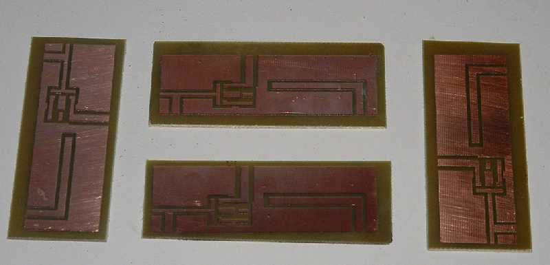
Since the board is small (1" X 3"), a number of them were processed in parallel on a single larger blank. The blank was then cut into individual pieces. The cut left the boards larger than needed. The first step in assembling the board is to trim it to the size of the top side copper field. All board material beyond the top side field must be removed.
I have learned that cutting PC boards can be difficult. Thick boards simply dull blades. Fiberglass and copper are tough materials, and often do not cut neatly. The danger with smaller boards is that the copper layer will be lifted off of the fiberglass substrate. This happens when the teeth on a blade grab the copper as opposed to cut the copper.
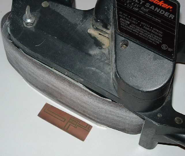
My favorite technique for trimming PCBs is sanding. Sitting down with a piece of sandpaper is time consuming and not very accurate. The better solution is to use a mechanical sander. This removes all of the elbow grease, makes a straight edge, and takes only a few seconds.
|
|
|
|
| Boards Before Trimming | Disk Sander On Shopsmith | Belt Sander Alternative |
The left picture shows four boards before trimming. The board material outside of the 1" X 3" copper rectangle must be removed. I put the disk sander attachment on my Shopsmith Mark 5. This provides a 12" flat sanding surface. The table is brought right up to the face of the sandpaper so that the board is fully supported and held perpendicular to the sander. A medium grit paper works well.
After the disk reaches the desired speed, I moved each of the 4 edges up to the sandpaper. As the material is removed, the remaining board appears as a line of material which is a different color than the copper. Adjust the angle of the board to keep the outer edges straight and parallel to the copper. Right at the point where the sanding is complete, the color of the edge changes, because the exposed fiberglass is completely removed. It's a definitive indication of reaching the stopping point.
If you don't have a disk sander with an accessory table, an alternative is a belt sander. While this works, the process is not as precise since it's harder to control the sander.
After the board is trimmed to size, any burrs on the edges can be removed with a standard flat file.
There is nothing wrong with using a hacksaw, or even better, a band saw. I just happen to prefer this method.
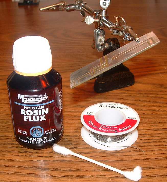
After being trimmed to size, the board should be tinned with solder. Tinning will keep air off of the copper, which retards oxidation, and tinning helps in the surface mount assembly process by providing a small amount of solder to tack down the first connection to a part.
Tinning is accomplished by first coating the surface of the clean board with liquid rosin flux. If the board is not clean, first use some fine steel wool to shine up the board, and be sure to remove all steel wool residue. Another alternative is the more abrasive scouring pads (NOT SOS, but like nonmetallic Scotch-Brite (tm)). The board can be tipped at an angle to reduce the chance of creating a pool of solder as opposed to a thin coating. Heat the board with a standard soldering iron. As the region under the iron comes up to temperature, solder will freely flow onto the board. I used a painting motion, moving the solder and the iron together, and covering the whole face of the board. Both the top and bottom of the board were tinned.
Here is a picture of the tinning set up.
 |
| Tinning Set Up |
The bottom of the board represents one plate of a large capacitor, working against the top of the board, with the fiberglass acting as the dielectric. In order to cancel that effect, the bottom of the board must be bonded to the top of the board.
There are two different approaches. According to Paul, N2PK, either approach works fine, but it is not necessary to use both.
The first approach involves drilling a series of holes at key points on the board and soldering wires between the top and bottom surfaces. This is the approach seen in the N2PK articles. Consult the documentation for the locations of the grounding wires.
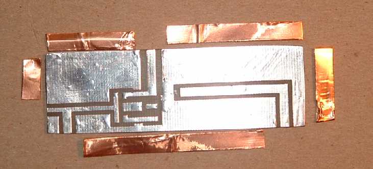
The second approach, the one that I used, bonds the bottom to the top using a copper foil which is run around the perimeter of the board, skipping the connector mounting points.
Assuming that you are working with the January, 2004 group build box, you will find a length of copper foil in the T1-6T bag. This foil has a sticky back which is protected with a backing tape. The foil is cut into 5 lengths which march around the perimeter of the board.
 |
 |
 |
| Board with Perimeter Bonding Foil | Leaving Space for the Connectors | Burnishing the Foil |
In the left picture, I've cut the tape and positioned the pieces next to the portion of the perimeter that they will cover. Gaps are left where the four connectors attach. Do not bring the bonding tape too close to the connector area, especially if you are planning on using SMA connectors.
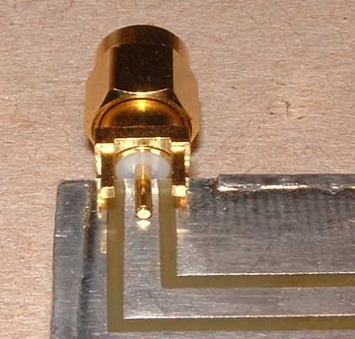
The middle picture shows an SMA connector pushed onto the board, and I do mean pushed. Normally, PCB SMA connectors are mounted perpendicular to the PCB. Five holes are drilled, four for the corner ground pins, and one for the center pin. These are soldered to the board to complete the connections. In this case, the connectors have been mounted in a clever manner, where they are parallel to the board. The channel between the center pin and two of the ground pins forms a slot which accepts the edge of the board. The connector is held firmly in place. The center pin lies on the signal trace, and is ultimately soldered to the board. The two ground pins are soldered on the bottom of the board. This configuration should have a minimal impedance bump, due to the short and smooth transition between the 50 Ohm board and the 50 Ohm connector.
The tolerances are very tight, and you do have to work to push the connector on the board in this orientation. If the bonding foil was in the area of the ground pins on the connector, it would be nearly impossible to press on the connector. I do not plan on using SMA connectors, but I still left that small gap between the end of the foil and the end of the copper on the board.
The foil should be evenly divided between the top and bottom of the board. The sticky back holds the foil in place while you are applying it, but when you have all of the pieces on the board, use a rounded, hard object to burnish the foil onto the board. I used the handle of my X-Acto knife, as shown in the right picture.
At this point, we really haven't done much to the electrical properties of the board, since the adhesive backing of the foil is preventing contact between the foil and the board faces. To remedy that situation, return to the solder and iron, and coat all of the foil/board junctions with solder. In fact, tin the entire exposed surface of the foil. The solder should transition off of the foil and onto the board. For this operation, I returned to my normal soldering iron (not the SMT iron) and standard rosin core solder. Be careful in the region of the board where two resistors mount near the edge of the board. Keep that area from getting clogged with solder. Clog it with resistors instead.
NOTE: If you employ edge bonding, you must still drill a single hole, and add a wire to bond the top to the bottom. This wire grounds a small rectangle of copper on the top of the board which helps maintain the traces as transmission lines. If you do not add this wire, the bridge will certainly work, but performance may be compromised.
 |
| Drilling the Ground Wire Hole |
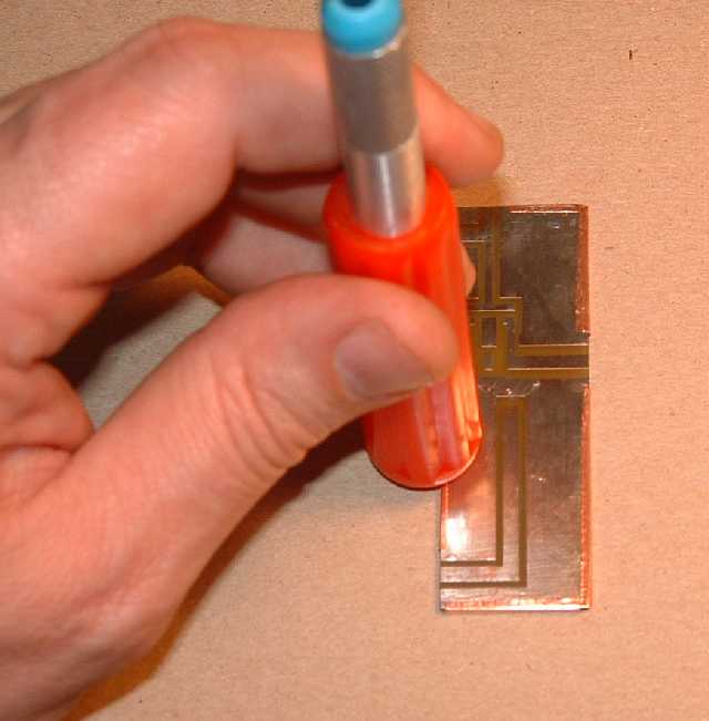
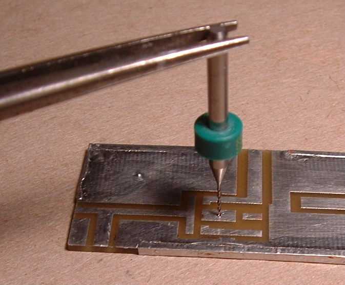
The rectangle in question is located next to the land which supports pin 2 of the T1-6T transformer. Another way to say it is that it is the only isolated island of tinned copper. The drill bit in the previous picture highlights the rectangle.
I used a small carbide drill to make a hole for 30 gauge wire wrap wire. The wire is folded over on each side of the board, and soldered in place.
After the board is sized, tinned, and bonded, it's time to add the components. We can leave metal shop and go back to the electronics lab.The components consist of 2 capacitors, 6 resistors, and a T1-6T transformer. If you are building your bridge following the January, 2004 group build, you need to get out three zip bags, numbers #011, #039, and #041. They hold the capacitors, resistors, and transformer, respectively.
Here is a picture of the parts and set up right before they were added.
 |
| Ready For Assembly |
My SMT assembly tools are described on another page. In order to get the right parts in the right locations, I refer to two different documents. Both are part of the various build info files on the N2PK VNA web page. A document entitled T1-6T Bridge Build Info.pdf has a number of layer drawings and several actual photos. What I also find useful is the bridge printed circuit drawing, in file T1-6T Bridge.pcb. In order to view this file, however, you will need to down load the free ExpressPCB layout editor software. I also have out the bridge parts list on the blue paper to provide a mapping between part number and bag number.
As mentioned at the top of this page, there are small differences between the board described in the documentation, and the board supplied with the January, 2004 group build. Resistors R1, R2, R3, and R4, are pulled left until they align vertically with the trace going to P1.
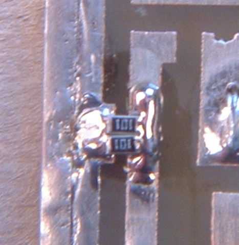
I chose to add the capacitors, then the resistors. The capacitors, part #011, are 8 pf NPO items in a 0805 package. These are the only two capacitors of that value in the VNA kit, so you should find exactly 2 parts in the #011 bag. The resistors are part #039. The kit includes 8 resistors, and 6 are used on the T1-6T board. The remaining 2 are reserved to construct a 50 Ohm load. Each resistor has a value of 100 Ohms, at 0.1%. Two resistors in parallel will create a precise 50 Ohm combination. The resistors are contained in the 0603 package, which is very small.
The capacitors just span the gap between ground and the signal. You have to center them in the gap. The capacitors appear to be located approximately 1/3 of the way from the right-angle turn on the trace to the end of the board. Here is a picture, on the left showing the placement of the capacitors prior to flux and solder.
 |
 |
| Capacitor Placement | Soldered Capacitors |
The picture on the right shows the capacitors after they are soldered in place. I first tack soldered the outer joints, then I did both center joints at the same time. After installing the capacitors, I checked that the signal trace was not shorted to ground. That's hardly a complete test, but probably good enough for this situation.
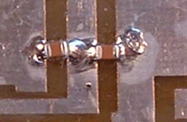
The resistors have their own challenges. First, they are in the 0603 package which is very small. On top of that, they are grouped into units of two, one right next to each other. This can be tricky, since solder tends to flow beyond the profile of the part, which means that it will get in the way of moving the second part right next to the first. I've tried various permutations on soldering the pairs, and nothing appears to be the clear winner. In any case, install the three pairs, R1-R2, R3-R4, and R5-R6. It is possible to Ohm out the pairs, but be sure to follow the traces to understand what value of resistance is correct between two points.
By the way, the resistors are labeled with 101 on one side, which I assume is the top side. That code indicates a 100 Ohm resistor.
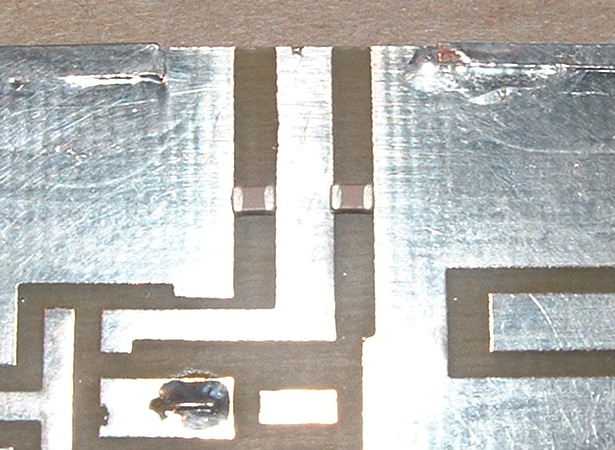
Part of the fun of this is trying to take very close-up pictures of very small parts. I found that I could put my 5X single-eye magnifying glass in front of my camera, while it was in macro mode. Here is a picture of two resistors (R5-R6), after soldering.
 |
| Two, 100 Ohm 0603 Package Resistors in Parallel |
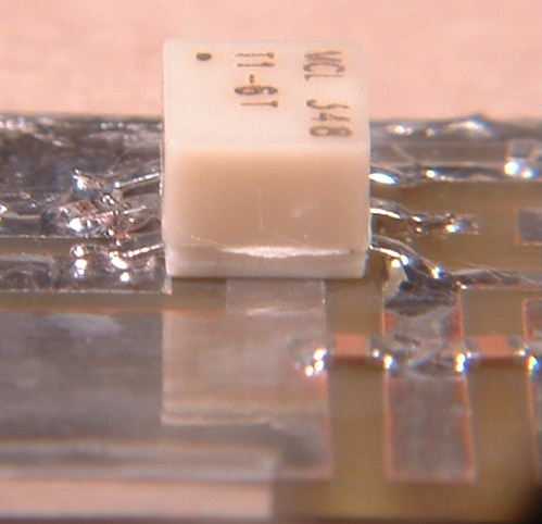
The transformer should be flush mounted to the PC board. Trim and bend the legs to keep them as short and direct as possible. Some T1-6T boards, due to the board material, will have a wider spacing between the traces. This complicates the lead bending. If necessary use a small length of jumper wire (#30 wire) to connect the lead stub to the board.
 |
| T1-6T Transformer |
I determined the placement of the part, and soldered as many legs as I could. That held the piece in place. I then used a dental pick to maneuver the remaining leads onto the traces.
Connectors and enclosures are up to you. The initial VNAs were built with SMA connectors, which are inexpensive and have a high frequency rating. An alternative is the N connector, which is my choice. Perhaps the only choice to avoid is the UHF connector, which does not maintain an 50 Ohm impedance through the connector. That impedance bump will add error to high frequency measurements.
The bridge to VNA interface is made with two connections. The pin to pin spacing between the RF DDS Out connector and the Det. RF In connector is 2.5 inches. The design intent was that the bridge board could be directly mated to the VNA enclosure. This creates a mechanically unified VNA/bridge, but yet the bridge can be replaced with other bridges or adapters. Examples of this can be found on the N2PK VNA web page, and VNA documentation. The bridge has male connectors, and the VNA enclosure has female connectors. This design also keeps the connections between the VNA and bridge very short, nothing more than the length of two mated connectors.
The trick to making this work is to be sure that the spacing between connectors on the bridge and on the VNA enclosure is exactly the same, since two connectors must mate at the same time. Even small variations in spacing will make the connectors difficult to mate, and can even lead to eventual failure due to the constant lateral stress. Since there will always be some variation in the hole spacing on the VNA due to drill wandering and the inherent mechanical tolerances, the best way to proceed may be to complete the solder connections between the bridge board and the bridge connectors only when the connectors are actually mated to your VNA. In other words, use the mated connectors as an alignment jig. Still, you cannot be too sloppy with the hole spacing on the VNA enclosure, since there is not that much wiggle room on the bridge board, perhaps 1/16" across both connectors.
The enclosure is described on another page.
The bridge is a great project for getting into SMT assembly. It can be assembled in about an hour. You can add the resistors, capacitors, and transformer without concern for the ultimate connector choice and packaging of the bridge.
Back to my Experimentation Page