 |
| Top Mask Corrections |
Greg Ordy
After being involved with two group builds, I'm left with a range of boards and parts. I'm making these available to aid those wanting to build their own VNA, and as replacement parts for a completed VNA.
The parts are mainly resistors and capacitors which were bought in larger quantities due to their relatively low costs. For example, the group might have needed 180 of some particular part, and the parts were sold in units of 100, with an additional price break at 200 parts. I bought 200 parts, and now have 20 remaining.
I have very few, if any, of the active devices, such as integrated circuits. In general, those were not bought in enough quantities to get into price breaks, and they were more expensive to begin with.
The prices of the parts are available on a spreadsheet which was used with the first group build. Go to the third table in the spreadsheet, and find the Replacement Cost column. This column contains your cost. Of course I'm only selling parts that I have on-hand. In order to find out if I have something here, you'll have to contact me. If you can't read spreadsheet files, please contact me and I'll email you a plain text copy. Added to each shipment will be the shipping costs, which should not be very much, unless you want some sort of expedited delivery.
I do have several Fox JITO-2 oscillators. These parts do reduce the dynamic range of the VNA somewhat. This is described on a page that I have, and one on the N2PK web site. Their good point is that they are much less expensive than the Valpey-Fisher part. The units I have cost $10, including shipping. Add a dollar for International shipping or PayPal.
Please contact me if you are interested in boards or parts. A link to my email address can be found on my home page.
I have a number of VNA printed circuit boards. These were made as part of the second group build. They are set up to accept the LTC2440 ADC, not the original LTC2410. This is a more capable part, since it can support 10 different conversion rates. The reason why the board was not used in the build was that there are several places where the solder mask incorrectly covers a small region of copper. There are three regions on the top of the board, and seven on the bottom. With about 2 minutes of scraping with a hobby knife the excess solder mask can be easily removed. I have built a working VNA from this batch of boards. They are high quality boards made of FR-4 material.
In order to use the LTC2440 chip, you will also need an extra pull-up resistor which is not part of the historic N2PK parts list. I used the value of 100K. It's in a 0603 package.
The cost of each board is $10 (USD). Add a dollar for International shipping or PayPal. That amount includes worldwide postage. If you want, I will remove the solder mask right before the board is shipped. Or, you can remove the solder mask yourself, when ready for assembly.
In order to put these changes into the proper context, please consult the N2PK build information, which includes detailed board pictures with parts annotations.
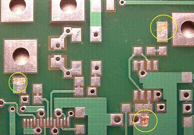
Here is a picture of the top side modifications.
|
|
| Top Mask Corrections |
The three modification areas are enclosed in yellow circles.
The left circle is at the bottom of R124, which is a 49.9 Ohm resistor. The resistor spans from the signal path to the ground around J120.
The lower middle circle is at the bottom of R153. It connects R153 to +5 VDC. This is perhaps the most confusing area on the board, where three resistors are located in an area which appears to be laid out for only two.
The upper right circle is above the top of R152. This area is the connection point for the cable at J150.
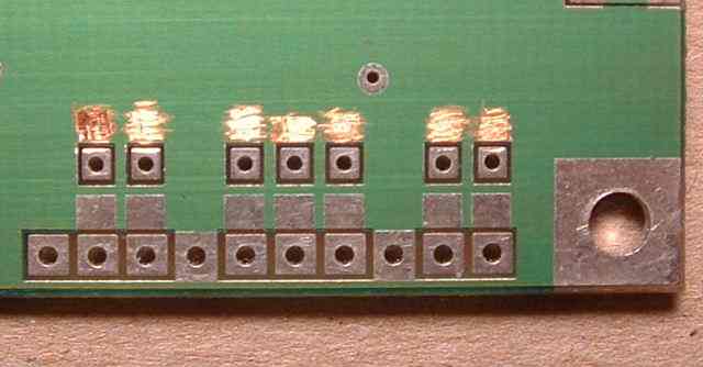
Here is a picture of the bottom side modifications.
 |
| Bottom Mask Corrections |
The bottom solder mask corrections are all related to the J160 plug. The 10-pin connector has 7 signal pins. Each pin has a resistor and capacitor in parallel which are attached to ground. These parts are stacked vertically on each other, and are located on the bottom of the board. The unmodified board has 7 ground pads which are located between the through holes and the connector. While this is correct electrically, the problem is that if the parts are placed towards the connector, the connector cannot seat down on the board. The parts should be grounded to the side opposite of the connector. In the above picture, the solder mask must be removed above the through hole pads. The ground pads right next to the connector pins are not used.
Back to my Experimentation Page